Skip to content
Nanomaterials and Nanoelectronics
Materials often exhibit exceptional electrical, optical, mechanical, and thermal properties at nanoscale. However, although these nanomaterials are attractive for certain applications, their adoption in practical technologies poses significant scientific and engineering challenges. We seek to understand these unique properties of nanomaterials, and further exploit their integration into nanoelectronic devices to realize better device performance, enhanced functionality, and new form factors. We target at problems ranging from material purification, self-assembly, device engineering and integration to push them from proof-of-concept demonstrations to real technologies.
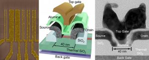
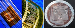
Flexible Electronics
Electronic devices are mostly made on rigid and brittle substrates like silicon wafers. However, in many Internet-of-Things and biomedical applications, we prefer the active electronics to be flexible or even conformal on irregular surfaces such as human body. We develop new materials and associated processing techniques to achieve this target, with focus on high-performance devices that are capable of performing edge-computing and wireless communications.
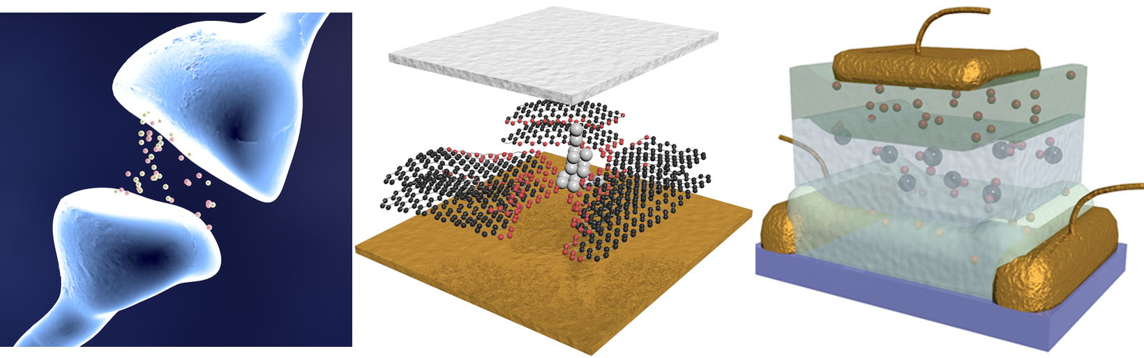
Next-Generation Memory Devices for Neuromorphic and In-Memory Computing
Machine-learning technology has made phenomenal progress in recent years. Such improvement comes with the cost of aggressively increased depth and size of the neural network models utilized, which leads to exponentially increasing computational load. A critical bottleneck is the slow and energy consuming data communication between the off-chip memory and the on-chip caches, as the scalability of the static random-access memory (SRAM) cache is insufficient for on-chip storing all of the data involved in the deep-learning algorithms. We develop new types of memory devices as “artificial synapses” in the next-generation neuromorphic deep-learning accelerators. They have potential to achieve on-chip storage with density and capacity high enough to eliminate the off-chip memory access, and enable fast and parallel in-memory analog computing to dramatically enhance the system’s efficiency to perform both the inference and the back-propagation training of deep neural networks.
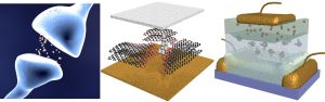
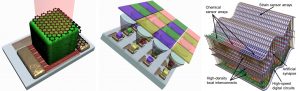
Heterogeneous Materials Integration
Assembly of dissimilar materials together is an important approach to enhance the performance and functionality of modern electronic and optoelectronic devices and systems. Here we explore the integration capability offered by the solution-based materials deposition process and the dry transfer-printing process to assemble different electronic materials monolithically on a common substrate. The target is to develop multispectral focal-plane photodetector arrays and 3D system-on-chip with integrated sensing, computation, memory, and communication functionalities.
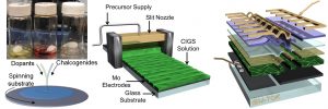
Solution-Processed/Printable Electronics
Electronic materials are typically deposited or grown in vacuum. However, these conventional thin-film material deposition techniques are not suitable for the deposition of materials with complex stoichiometry uniformly over large area. We develop novel chemistry for the deposition of high-quality inorganic electronic materials from their solution precursors. Such solution-based process not only greatly improves the throughput and reduces the capital cost for equipment, but also enables better control over the composition and doping of a variety of chalcogenide-based electronic materials for applications ranging from thin-film transistors, memories, to photovoltaics.